
What Does Nexus Photonics, Acquired by IonQ, Actually Build?
The Company Turning Quantum-Computer Optical Systems into Chips

Introduction
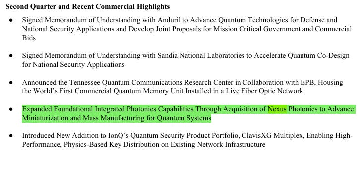
In IonQ’s second-quarter 2026 results announced today, one item stood out beyond the revenue growth itself.
IonQ completed the acquisition of Nexus Photonics, stating that it had secured the core integrated-photonics capabilities needed for quantum-system miniaturization and mass manufacturing.
Nexus Photonics is not simply a component supplier that delivers optical parts.
It is closer to a company that can integrate lasers, modulators, converters, detectors, low-loss waveguides, and filters — all optical building blocks needed for quantum computers and quantum sensing — into a single photonic integrated circuit, or PIC.
In particular, from IonQ’s perspective, this acquisition does not merely mean “a smaller optical network.”
It may mean compressing the complex optical systems used for ion cooling, initialization, gates, and measurement into chips.
In this article, I will look at what technologies Nexus Photonics owns, why a small company could participate repeatedly in DARPA and U.S. defense projects, and what role it may play inside IonQ’s photonics strategy when combined with Lightsynq, Oxford Ionics, Vector Atomic, and SkyWater.
What Kind of Company Is Nexus Photonics?
Nexus Photonics is not a company that builds full quantum computers based on photonics.
It is a photonic integrated circuit company that integrates optical components needed for quantum computers and quantum sensing into one optical chip.
In other words, it is a company that compresses optical elements — lasers, frequency combs, converters, detectors, filters, and passive waveguides — that would otherwise sit separately on an optical table into a semiconductor-chip-level platform.
IonQ announced in its second-quarter 2026 results that it had completed the acquisition of Nexus and described it as a core integrated-photonics capability for quantum-system miniaturization and mass manufacturing.
Company Overview
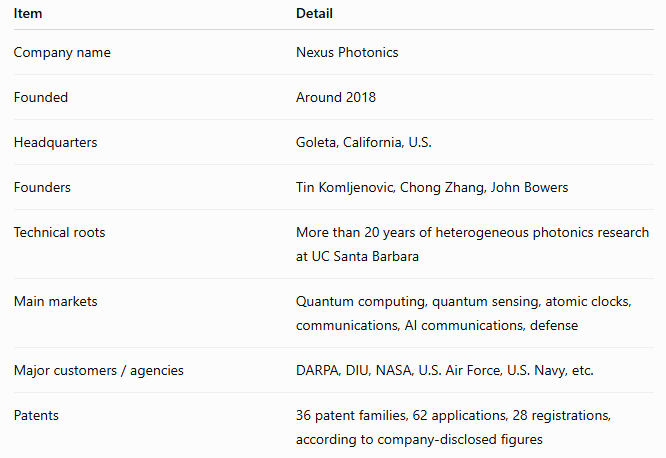
Based on publicly available SBIR materials, the company appears to have around 15 employees.
In other words, this is not a manufacturing company on the scale of thousands of employees like SkyWater.
It is closer to a deep-tech company that owns a small number of highly sophisticated photonic-process IP assets.
One important point is that co-founder John Bowers is one of the leading silicon-photonics and heterogeneous-photonics researchers at UCSB.
He is also connected to companies such as Aurrion and Aerius Photonics, and his research group has produced several related photonics startups.
So Nexus is better understood not as a simple university spinout, but as a company commercializing the long accumulation of UCSB Bowers Lab’s integrated-photonics technology.
UCSB is also known as a representative institution cooperating with Cisco in quantum-networking research.
Nexus’s Core Technology: Heterogeneous Photonic Integration
The core of Nexus is heterogeneous photonic integration.
In building a photonic chip, one material cannot perform every role well.
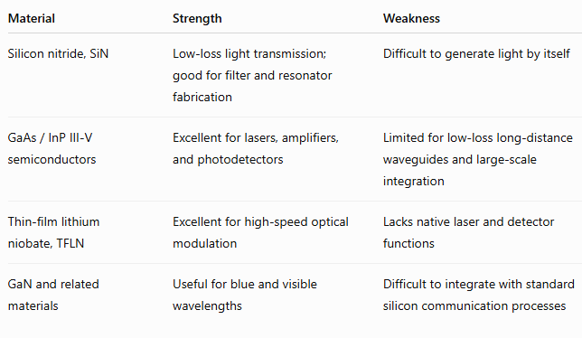
Instead of packaging these materials separately, Nexus combines an SiN waveguide with III-V materials such as GaAs and InP, and when needed, also combines TFLN.
As a result, the following functions can be integrated on one chip.
Low-loss waveguides
On-chip lasers
Optical amplifiers
Photodetectors
Optical filters and couplers
High-quality resonators
Frequency combs and multi-wavelength light sources
Nexus explains that its platform supports a complex wavelength range from roughly 400 nm to over 1,700 nm.
This is important because, compared with general silicon photonics that is concentrated around the 1,310 nm and 1,550 nm telecom bands, quantum and atomic transitions often require visible and near-infrared wavelengths.
Technical Knowledge: SiN and III-V
SiN: The Road That Carries Light
SiN stands for silicon nitride.
SiN is very useful as a waveguide that carries light inside a chip.
Its advantages include:
Very low optical loss
Ability to handle broad wavelengths from visible to near-infrared
Ability to build very high-quality resonators
Compatibility with wafer-level manufacturing
Suitability for large-scale complex optical circuits
However, SiN is not a good material for generating light efficiently through electrical injection.
So SiN is excellent as a road for light, but weak as a laser material.
III-V: The Material That Creates Light
GaAs means gallium arsenide.
InP means indium phosphide.
Both are III-V compound semiconductors.
These materials have a direct bandgap, meaning they can efficiently generate light when electrons are injected.
They are therefore strong for:
Lasers
Optical amplifiers
Photodetectors
High-speed optical devices
However, building broad and complex optical circuits only with III-V materials can create problems such as higher propagation loss, manufacturing cost, circuit size, and yield.
So the role division is this:
SiN creates the low-loss optical road.

GaAs or InP is attached only where light generation or amplification is needed.
Why Ordinary Silicon Photonics Alone Is Not Enough for Quantum Technology
Optical communication chips for AI data centers mainly use 1,310 nm or 1,550 nm.
But atomic and ion-based quantum systems require lasers with wavelengths specific to each atom.
For example, Ba⁺ ions use precise light around:
About 493 nm:
used for cooling and state detection

About 650 nm:
used for repumping
IonQ uses barium ions, and has explained that this is favorable for standard photonic devices and networking because barium uses visible optical wavelengths.
Nexus’s broad 400–1,700 nm-class platform includes these barium visible wavelengths.
Therefore, Nexus is not simply supplying IonQ with a data-center communication chip.
It provides laser-system integration capability that can control and read out barium ions.
However, IonQ has not publicly disclosed exactly which laser lines or which generation of QPU Nexus chips will be applied to.
The above interpretation is based on the possible use cases that can be inferred from the combination of the technologies.
What Is Different from Existing Systems?
Current quantum-computer and atomic-clock systems often have a large structure.
Laser
→ optical amplifier
→ frequency stabilization device
→ converter
→ switch
→ optical fiber
→ vacuum chamber
Each device is often connected separately through optical fiber or free-space optics.
This structure has several problems.
Too many parts
Precise optical alignment is required
The footprint is too large
Component phase drift occurs
Assembly and calibration take a long time
Each system requires manual tuning
Nexus’s goal is to turn this large optical delivery system into an application-specific PIC, or a customized photonic integrated circuit for quantum-systems use.
Nexus has described this direction in DIU projects as replacing a bulky optical table made of lasers, mirrors, amplifiers, detectors, switches, and passive optical components with a single semiconductor chip.
In other words, the goal is not only to put the QPU’s ion trap onto a semiconductor chip.
It is to semiconductorize the light source and optical front end that move, prepare, and measure ions.
Especially Important Technology: Ultra-Quiet Lasers and Phase Stability
Nexus’s key product line includes not only general lasers, but ultra-low-noise lasers and ultra-quiet lasers, meaning lasers with very low linewidth and phase noise.
In quantum computers, atomic clocks, and quantum sensing, even small laser fluctuations create problems.
Atomic-transition frequency and laser frequency can drift apart.
Ion cooling efficiency can fall.
Gate phases can drift.
Interference visibility can decrease.
Optical phase formation and signal reading can become harder.
The precision of atomic clocks and sensors can degrade.
Nexus combines low-loss, high-quality SiN resonators with III-V lasers, attempting to shrink optical-bench-level low-noise performance to chip size.
The company calls this technology an ultra-quiet chip-scale laser.
This is directly connected to optical frequency combs, phase synchronization, and distributed quantum-system infrastructure.
In that sense, Nexus is not merely a QPU-component company.
It is closer to a company that can chip-scale the optical engine needed to stabilize the frequency and phase of quantum networks.
Major Government Projects
The reason Nexus is technically notable is that DARPA, DIU, and NASA have repeatedly assigned projects to the company.
DARPA LUMOS
In 2020, Nexus was selected for DARPA’s LUMOS program.
The goal was to create lasers with precisely designed wavelengths, not limited to telecom wavelengths but extending into visible and near-infrared regions.
In 2024, Nexus received additional commercialization and scale-up expansion contracts after Phase 3.
This means the project is moving beyond proof of concept and toward production and commercialization.
DARPA GRYPHON
In 2022, Nexus was selected for the GRYPHON program to develop low-phase-noise photonics-based frequency synthesizers.
The goal was to implement lower phase noise than existing individual oscillators in a small form factor.
This is connected not simply to 5G or 6G, but also to precision time, radar, RF photonics, and quantum sensing.
DIU Quantum Sensing
In 2025, DIU awarded Nexus a contract to significantly reduce the size, mass, volume, and cost of quantum sensors.
The core idea is to integrate lasers and optical components needed in current atomic sensing systems into one integrated photonic platform.
This can be applied to:
Atomic clocks
GPS-denied PNT
Magnetometers
Gravity sensors
Inertial sensors
DARPA INSPIRED
In 2025, Nexus participated in a next-generation optical detector development program together with UCSB, Caltech, MIT, and the University of Virginia.
This is a project that uses SiN and III-V materials to generate squeezed light and connect it to high-efficiency detectors that can be integrated on a chip.
Squeezed light is a core technology that can improve sensing beyond the standard quantum limit.
Besides these, the company has also participated in NASA’s THz detector work, U.S. Air Force wearable optical laser work, and IARPA atomic-clock projects.
Why Nexus Could Win Repeated Defense, DARPA, and Research-Lab Projects
There are several reasons Nexus has repeatedly received government and research contracts.
First, the problem itself matches a military and national-lab bottleneck.
DARPA and the U.S. government do not only fund large companies.
Second, Nexus has a small team, but its technical density is high.
Nexus is based on more than 20 years of heterogeneous-photonics research from UC Santa Barbara and the Bowers Lab.
Key people include:
Tin Komljenovic:
Nexus CEO; participated in multiple DARPA heterogeneous-photonics programs from the company’s beginning

Chong Zhang:
researched integrated photonics at HPE and holds more than 100 papers and patents

Minh Tran:
formerly at Aerius and Xtera; researcher in photonics design, optical amplifiers, and lasers

John Bowers:
UCSB professor, world-class integrated-photonics researcher, co-founder of Aurrion and Aerius Photonics, and previously connected to Juniper and FLIR acquisitions
Third, Nexus already had proof that contracts could become real outcomes.
Nexus is not simply good at writing proposals.
In 2020, it demonstrated electrically pumped GaAs-on-SiN lasers at wafer scale.
In 2022, a Nature paper demonstrated fully integrated PICs that combine III-V gain elements, SiN waveguides, and passive components within a 1 μm-thick photonic layer.
This is evidence that the core devices actually work, not only that they are theoretically possible.
Fourth, its technical requirements matched defense needs precisely.
For commercial silicon photonics, the required wavelengths are usually optimized around 1,310 nm and 1,550 nm.
DARPA LUMOS was created to solve the problem that existing commercial photonics could not provide those special wavelengths and performance.
Especially in visible and near-infrared wavelength ranges, the goal was to create lasers with a wavelength-by-design approach and transfer them into a structure that could be manufactured by a foundry.
Nexus’s technology matched this requirement very closely.
Nexus’s Differentiation
Many photonics companies can perform individual functions that Nexus targets.
But not many companies can implement the full target set using the same material platform, the same chip, and a broad wavelength range all at once.
The requirements Nexus is trying to satisfy at the same time are:
1. Wavelengths that atomic systems actually need
The telecom industry is mostly concentrated around 1,310 nm and 1,550 nm.
But ion traps, neutral atoms, and atomic clocks each require different visible and near-infrared wavelengths.
2. Light generation inside the chip
Just because a data-transmission laser works well does not mean it is enough for high-fidelity quantum gates.
If the laser linewidth is broad or the phase fluctuates, state preparation and gate accuracy can fall.
Nexus’s III-V / SiN laser has demonstrated linewidth down to around the 980 Hz level.
3. Integration of active and passive components at the same time
Combining separate components from other suppliers can still make a system.
For example:
Company A laser
+
Company B modulator
+
Company C detector
+
Company D SiN chip
+
Company E packaging
But as the number of parts grows, insertion loss, coupling loss, noise, thermal drift, connector failure, assembly cost, and lead time increase.
Nexus’s goal is to monolithically or heterogeneously integrate these elements.
Laser
+
modulator
+
filter
+
detector
+
waveguide
+
resonator
all inside one PIC.
4. Direct co-design with IonQ
The difference between buying parts from a commercial photonics vendor and keeping a photonics team inside the company is large.
IonQ did not acquire Nexus simply because “nobody else can make this.”
The reason appears closer to this:
IonQ wants to avoid being forced to wait for external suppliers to decide the priorities and volume economics of special wavelengths needed for future QPUs.
Instead, it wants to co-design them directly into IonQ’s own roadmap.
What Nexus Provides to IonQ
1. Miniaturization of Optical Systems for Quantum Computers
For ion-trap quantum computers, the expansion bottleneck becomes not only the number of ions, but also the laser channels and optical-control systems.
Potentially, Nexus’s PICs can integrate the following functions at chip level.
Ion-cooling light sources
State-preparation light sources
State-readout light sources
Frequency and phase stabilization
Beam routing and switching
Optical broadcasting across multiple QPU zones
Therefore, the likely goal is not to reduce the size of a single quantum computer, but to manufacture identical optical modules repeatedly and mount them on many QPUs.
2. Strong Fit with Barium QPUs
Nexus’s broad-wavelength platform aligns well with the visible wavelengths of barium ions that IonQ has adopted.
One reason IonQ chose barium was to improve usability with standard photonic devices and networking.
Nexus pushes this advantage one step further by providing the foundation to build barium optical systems at chip scale.
3. Photonic Interconnect Manufacturing
Lightsynq uses diamond-based quantum memory, especially SiV color centers.
The core of Lightsynq is storing photons in memory, confirming successful storage, and performing Bell-state measurement and entanglement exchange inside the memory.
In the Boston research lineage, nanophotonic experimental equipment was used to test such diamond PIC and interconnect systems.
Lightsynq has already shown the direction of putting diamond membranes onto one chip.
Nexus is responsible for the lower-level optical hardware layer.
It creates, amplifies, stabilizes, guides, and sends light through the desired path inside the chip, and finally detects it.
Nexus publicly explains that it combines lasers, amplifiers, detectors, converters, waveguides, filters, and resonators over a range from roughly 400 nm to more than 1,700 nm.
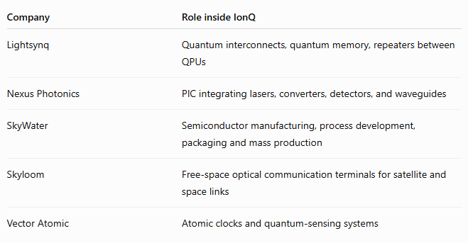
Therefore, Lightsynq is closer to the layer that decides what to connect and how to transmit entanglement, while Nexus is closer to the layer that implements those optical functions on a chip.
The expected actual connection flow could look like this:
1. IonQ’s ion QPU emits a photon entangled with a qubit.
2. A Nexus-family PIC controls the photon’s frequency, phase, timing, and path.
3. If needed, wavelength conversion or optical switching occurs.
4. The photon enters Lightsynq diamond memory or reaches another quantum path.
5. Lightsynq’s memory node stores the quantum state.
6. After successful storage is confirmed, entanglement with another QPU is established.
7. Multiple QPUs operate as one larger logical system.
So in real commercial quantum-networking, Nexus’s role is not limited to moving photons emitted by qubits.
It may become the optical engine that sends light toward the qubit, prepares the ion, controls it, measures it, and supports the entire quantum-computer optical stack.
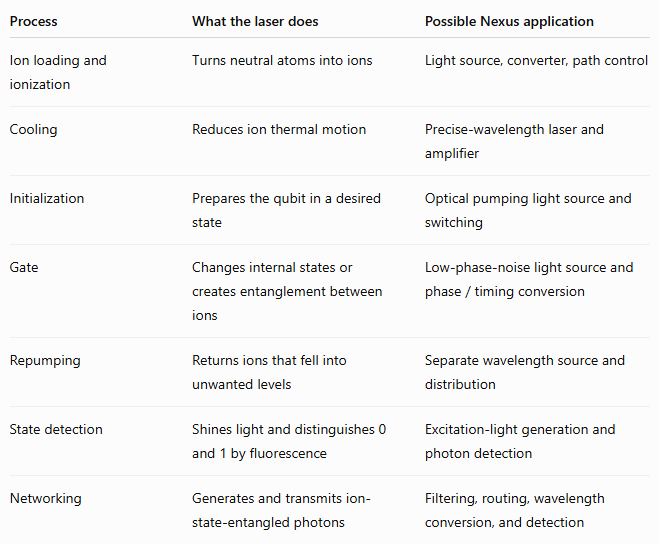
4. Wavelength Conversion for Quantum Networks
IonQ has already demonstrated technology that converts visible photons interacting with barium ions into telecom wavelengths suitable for long-distance optical-fiber transmission.
Nexus’s broad wavelength range, nonlinear photonics, and integrated lasers, converters, and detectors are exactly the type of platform that can chip-scale this visible-to-telecom conversion device.
However, it has not been publicly announced that Nexus directly handles this specific frequency-conversion module for IonQ.
5. Atomic Clocks and PNT
Nexus officially presents low-noise laser PICs for uses such as:
Atomic clocks
Quantum sensors
Quantum computers
Frequency synthesizers
RF photonics
Therefore, combining Vector Atomic’s atomic-clock and PNT systems with Nexus’s integrated lasers is also a natural direction.
The atomic cell or vacuum system inside an atomic clock would be handled by Vector Atomic, while the precise lasers and optical front end could be miniaturized by Nexus.
The Meaning Becomes Larger When Combined with SkyWater
Nexus itself does not appear to operate a huge semiconductor fab.
Based on publicly available materials, Nexus’s focus is on:
PIC design
Heterogeneous bonding process
Wafer-scale process development
Automated testing
Die separation
Advanced packaging design
Mass-production transition know-how
In other words, it is closer to a company that owns the device design and manufacturing recipe.
When SkyWater is added, the structure becomes more complete.
Nexus:
Designs the custom PIC modules IonQ needs

Lightsynq, Vector Atomic, and IonQ:
Define the required optical-function system specifications

SkyWater:
Turns wafer processes, packaging, and testing into actual mass production
IonQ has not yet specifically announced the exact production roadmap for this integration, but based on the public capabilities of each company, this appears to be the most natural direction.
Company Limitations and Items to Check
Nexus owns very important technology, but there is no need to exaggerate.
Items that have not yet been confirmed include:
The exact acquisition price IonQ paid
Nexus’s annual revenue
Actual production volume
Yield and production cost
Output per unit wafer
The first product to be applied to IonQ QPUs
Specific timeline for transfer into SkyWater production
Long-term reliability of 400 nm-region visible PICs
Radiation certification for space and defense environments
Manufacturing cost of visible, near-infrared, and telecom multi-wavelength integrated PICs
IonQ’s second-quarter announcement only stated that the acquisition had been completed.
It did not provide acquisition price or detailed financial information.
Also, making a PIC work and producing tens of thousands or hundreds of thousands of units at high yield are very different problems.
Therefore, the value of the Nexus acquisition may be determined less by the technology itself and more by whether IonQ can transfer it into SkyWater processes and succeed in repeatable production.
Conclusion
Nexus Photonics’s core value is not simply that it is a “laser company.”
It owns technology that can turn the complex optical systems needed for quantum computers, quantum sensing, and atomic clocks into mass-producible semiconductor chips.
From IonQ’s perspective, Nexus connects several areas at once.
Miniaturization of laser and optical systems for barium QPUs
Deepening of Lightsynq photonic interconnects
Miniaturization of optical front ends for Vector Atomic atomic clocks and sensors
PIC mass production through SkyWater
The most important point is that Nexus is not an acquisition that changes IonQ’s physical qubit technology itself.
Rather, it is a bottleneck-solving acquisition that may change the optical equipment, which has been blocking system expansion, into a chip.
If Oxford Ionics chip-scales ion traps and control electronics, Nexus chip-scales lasers and optical systems, and SkyWater manufactures them, then IonQ’s stated direction of miniaturization and mass manufacturing for quantum computers begins to connect as one structure for the first time.
Appendix
How Are They Actually Attached?
“Attaching on top” does not mean placing two finished chips on top of each other mechanically.
More accurately, the process is as follows.
1. First, make the SiN waveguide
A SiN layer is formed on the wafer, and microfabrication creates waveguides, splitters, filters, and resonators.
2. Separately prepare the III-V material
On a GaAs or InP wafer, a very thin semiconductor layer needed for lasers and amplifiers is prepared.
Then it is precisely transferred onto the desired location on the SiN wafer using methods such as:
wafer bonding
die-to-wafer bonding
micro-transfer printing
3. Create the electrical and optical structure in the III-V region
The bonded area is etched and metal electrodes are formed so electricity can flow.
That region then functions as a laser or optical amplifier.
4. Couple the light into the SiN waveguide
III-V produces light, and the light enters the SiN waveguide.
The optical modes of the two materials are designed to overlap very closely.
Usually, evanescent coupling through a gradually changing taper is used.
The idea is not that light suddenly jumps from one side to the other.
Rather, it gradually moves from the III-V region into the SiN region.
Conceptually, the structure looks like this:
Electrical input
↓
[GaAs / InP laser]
↓
bonded active material
↓ optical coupling
[SiN waveguide]
↓
light generation → amplification → filtering → conversion → distribution → detection
In Nexus’s detailed 2022 Nature paper, a dual-material PIC with lasers, amplifiers, detectors, converters, and passive waveguides was demonstrated in a photonic layer of less than 1 μm thickness.
The important point is that laser output was delivered to the SiN waveguide and integrated all the way to amplifiers and detectors.
Why Use Both GaAs and InP?
Because the required wavelengths are different.
The rough division is:
GaAs family:
Useful for visible and short near-infrared wavelengths

InP family:
Useful for telecom wavelengths around 1,300 nm and 1,550 nm

GaN family:
Useful for blue and ultraviolet light

SiN:
Base platform that carries light with low loss over a broad wavelength range
Nexus publicly presents a structure that combines SiN with materials such as GaN, GaAs, and InP, with the overall platform covering everything from blue light to infrared light.
TFLN, or thin-film lithium niobate, has properties where the refractive index changes rapidly and linearly when voltage is applied.
This makes it highly useful for high-speed phase and frequency modulation.
The typical materials shown in the hybrid platform Nexus has developed are mainly:
SiN
GaN
GaAs
InP
What Is a III-V Compound Semiconductor?
A III-V compound semiconductor is a compound semiconductor made by combining elements from groups III and V of the periodic table.
In older group notation:
Group III:
Ga, In, Al, etc.

Group V:
As, P, N, etc.
These elements are combined one by one to create different materials.
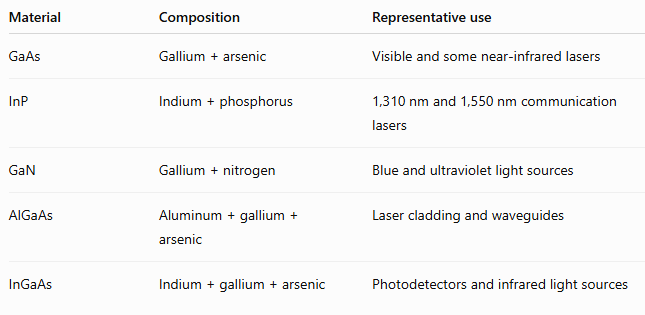
Silicon is a group IV semiconductor, made from one element.
But III-V semiconductors combine two different elements.
Why Are III-V Materials Better for Lasers?
In a laser, electrons must release energy as light when they move from a high-energy state to a lower-energy state.
GaAs and InP families have a direct bandgap, meaning electrons and holes can combine and emit energy as light very efficiently.
That is why they are used to make lasers and optical amplifiers.
By contrast, silicon and SiN are excellent for transmitting light, but weak at generating light efficiently through electrical injection.
So the conclusion is:
III-V creates and amplifies light.

SiN carries, distributes, and filters that light with low loss and high precision.
In Nexus’s Nature paper, GaAs / AlGaAs-family gain materials were bonded onto a SiN wafer to implement lasers, amplifiers, detectors, converters, and passive waveguides on one platform.
Why Are Wavelengths Different Even Within III-V Materials?
Even among III-V materials, the wavelength changes depending on the composition.
If the material composition changes, the bandgap energy changes.
The wavelength of the emitted light also changes.
GaAs family:
Relatively high energy, suitable for shorter wavelengths

InP family:
Suitable for telecom near-infrared wavelengths

GaN family:
Suitable for blue and ultraviolet wavelengths
By changing the ratios of elements such as In, Al, and Ga, and by changing quantum-well thickness, the desired wavelength can be designed more precisely.
This is also the meaning of DARPA LUMOS’s phrase “wavelength by design.”